
Most Popular


-
6
Actor’s excessive airport security sparks probe into human rights violations

-
7
Actor Yoo Ah-in accused of sexual attack

-
8
Man who let his father die due to financial difficulties to be released on parole

-
9
S. Korea, China shifting from tensions to cooperation: Seoul

-
10
LG Electronics achieves record earnings in Q2


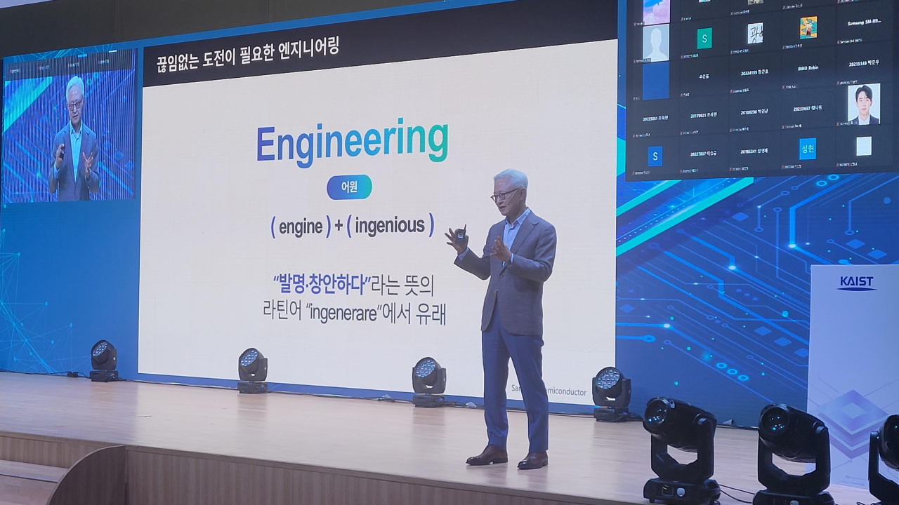
Samsung Electronics co-CEO Kyung Kye-hyun, who oversees the tech giant’s chip business, unveiled the company's five-year plan to develop memory chip-centered supercomputers and catch up with its Taiwan-based foundry rival TSMC.
Kyung visited the Korea Advanced Institute of Science and Technology in Daejeon, South Chungcheong Province, on Thursday to deliver a special lecture to promising talents. It was the first time Kyung delivered a lecture to students since taking office as co-CEO in December 2021.
During the lecture, the co-chief highlighted that the world's largest memory chipmaker’s goal is to create a technology that does not exist in the world. He also shared Samsung’s vision to build supercomputers.
“The Samsung Advanced Institute of Technology is trying to build a memory-centric supercomputer by 2028, but there is no one in the country who has designed ... (such) powerful computing devices,” the chip chief said.
Picking supercomputers as one of its future growth goals for chips, the tech giant has started stepping up its investment in research and development. However, it was the first time the company officially hinted at a target launch year for its supercomputers.
Samsung also set a goal to outperform TSMC, the world’s top foundry operator, within five years, while admitting that the South Korean tech giant’s foundry technology “lags behind TSMC” -- about two years behind in 4-nanometer process technology and a year behind in 3-nanometer process technology.
Kyung is positive about the goal since Samsung’s latest 3 nanometer chips have been built on the Gate-All-Around (GAA) technology since last June -- an industry first across the world. It allows up to a 45 percent area reduction while providing 30 percent higher performance and 50 percent lower power consumption, compared with the existing FinFET process that has been used for TSMC’s 3 nanometer foundry process.
TSMC will not use GAA before it reaches 2 nanometer production and Samsung believes this will allow the firm to catch up with its Taiwanese rival.
When asked about the impact of the US-China rivalry on Samsung, the co-CEO said: “While approval is required for investment in our Chinese plants in Xian, there has not been significant pressure on our overall business. … We’ll strive to turn the crisis into an opportunity.”
Samsung runs a chip manufacturing plant in the Chinese city of Xian, which is responsible for some 40 percent of Samsung's global NAND flash production. In Suzhou, the chipmaker operates a semiconductor packaging factory.


![[Today’s K-pop] Treasure to publish magazine for debut anniversary](http://res.heraldm.com/phpwas/restmb_idxmake.php?idx=642&simg=/content/image/2024/07/26/20240726050551_0.jpg&u=)