

Initial supplies slated for Nvidia, AMD as early as next month
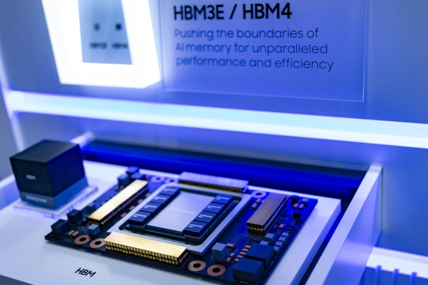
Samsung Electronics could begin mass production of its next-generation HBM4 memory chips as early as next month, with initial shipments expected to go to major customers such as Nvidia and AMD, according to industry sources on Monday.
The move could mark a turning point for Samsung in the high-bandwidth memory market for artificial intelligence, where it has lagged behind smaller rival SK hynix in recent years.
Industry observers say Samsung’s effort to narrow the gap hinges on a bold decision to adopt a sixth-generation 10-nanometer (1c) DRAM process — an industry first — despite weak early yields. The company also applied a more advanced 4-nanometer foundry process to the logic die, which functions as the control unit of the memory stack.
According to the sources, Samsung recently passed final qualification tests conducted by Nvidia and AMD and is now preparing to start mass production next month. The HBM4 chips are expected to be used in next-generation AI accelerators slated for release in the second half of this year, including Nvidia’s Rubin platform and AMD’s MI450.
The development comes as leading AI chip customers have reportedly revised their qualification benchmarks, raising speed requirements while easing thermal limits — effectively prioritizing raw performance over operating temperature margins.
Industry insiders said the changes followed recent advances in custom AI accelerators, including Google’s tensor processing units, which last year demonstrated AI performance comparable to or exceeding that of Nvidia’s GPUs.
In the latest qualification tests, Samsung’s HBM4 chips achieved data transfer speeds of 10.7 gigabits per second, meeting Nvidia’s requirement of 10 Gbps, according to an industry expert who requested anonymity. By comparison, SK hynix and Micron Technology recorded speeds of about 8.3 Gbps and around 8 Gbps, respectively.
“The shift in market demand raised the bar for speed while allowing higher operating temperatures,” the expert told The Korea Herald. “Samsung’s decision to push ahead with the 1c DRAM process, despite very low initial yields, appears to have been critical in achieving the required performance.”
The results were obtained under full-scale testing, the expert added, noting that smaller test batches can sometimes produce higher benchmark scores.
Previously, Samsung said its HBM4 chips achieved data transfer speeds of up to 11.7 Gbps. SK hynix, which announced the industry’s first development of HBM4 chips in September last year, has also said its product reached speeds of up to 11.7 Gbps.
For Samsung, combining the 1c DRAM process with a 4-nanometer logic die produced by its in-house foundry provided greater design flexibility in through-silicon via density and routing, enabling higher input and output speeds, the expert said.
By contrast, SK hynix’s HBM4 uses a fifth-generation 10-nanometer (1b) DRAM process and a 12-nanometer logic die manufactured by TSMC.
Following the latest qualification tests, SK hynix has reportedly redesigned its HBM4 chips while maintaining the same 1b process node and is now awaiting the results of renewed evaluations, industry sources said.
Both Samsung and SK hynix are scheduled to announce their fourth-quarter earnings on Thursday, when they are expected to provide updates on HBM4 orders and customer demand.
The timing is critical for memory suppliers. Nvidia CEO Jensen Huang said earlier this month that the company’s next-generation Vera Rubin platform is already in “full production” ahead of its launch in the second half of this year.
herim@heraldcorp.com