
Memory giant plans early shipments for Nvidia’s next-generation AI platform Vera Rub later this month
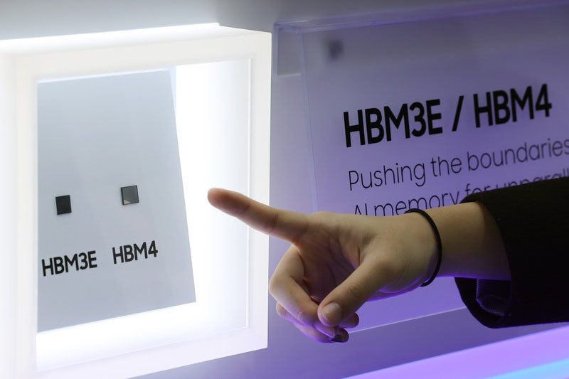
Samsung Electronics will begin shipments of its next-generation high bandwidth memory, HBM4, after the Lunar New Year holiday, becoming the first memory maker to commercialize what is widely seen as a game-changing chip for AI computing, industry sources said Sunday.
Samsung plans to start shipping HBM4 to Nvidia as early as the third week of February, for use in the US chip giant’s next-generation AI accelerator platform, Vera Rubin.
The move marks a strategic rebound for Samsung, which had faced questions over its competitiveness in earlier HBM generations. With HBM4, Samsung is seeking to close the gap with — and potentially move ahead of — crosstown rival SK hynix, which gained an early lead amid surging demand from AI data centers.
“Samsung has demonstrated a recovery in its technology leadership by being the first to mass-produce the highest-performance HBM4,” an industry official said.
“That gives the company a clear edge in shaping the market on its own terms.”
Nvidia is expected to unveil Vera Rubin accelerators incorporating Samsung’s HBM4 at its annual developer conference, GTC 2026, scheduled for next month. Samsung said the shipment timing was decided after coordination with Nvidia’s product roadmap and downstream system-level testing schedules.
Beyond speed, Samsung’s technological approach behind the product is also notable. From the outset, the company aimed to exceed standards set by JEDEC, adopting the industry’s first combination of a sixth-generation 10-nanometer-class DRAM (1c) process with a 4-nanometer logic die produced through its own foundry.
As a result, Samsung’s HBM4 delivers data transfer speeds of up to 11.7 gigabits per second, well above JEDEC’s 8 Gbps standard. The figure represents a 37 percent improvement over the standard and a 22 percent gain over the previous HBM3E generation.
According to sources, memory bandwidth per stack reaches up to 3 terabytes per second — roughly 2.4 times higher than its predecessor — while a 12-high stacking design enables capacities of up to 36 gigabytes. With a future 16-high configuration, capacity could expand to as much as 48 GB, industry estimates show.
Despite adopting cutting-edge processes, Samsung has achieved stable yields ahead of mass production, with further improvements expected as output scales up, sources said.
Samsung also emphasized power efficiency, noting that HBM4 is designed to maximize computing performance while reducing energy consumption, helping data centers lower electricity use and cooling costs.
The company expects its HBM sales volume this year to more than triple from a year earlier and has decided to install additional production lines at its Pyeongtaek Campus Line 4 to expand capacity. The P4 facility is planned to produce roughly 100,000 to 120,000 wafers per month, dedicated to 1c DRAM used in HBM4 products, industry sources said.
By last year, Samsung had already built monthly capacity of around 60,000 to 70,000 wafers for the 1c DRAM process. With the planned expansion, total 1c output earmarked for HBM4 would rise to about 200,000 wafers per month, accounting for roughly a quarter of Samsung’s total DRAM production capacity of approximately 780,000 wafers.
The HBM4 market is expected to be dominated by Samsung and SK hynix, with US-based Micron Technology effectively out of the race. According to market tracker SemiAnalysis, SK hynix is estimated to take about 70 percent of the HBM4 market, while Samsung is expected to account for the remaining 30 percent.
herim@heraldcorp.com