
Most Popular
-
1
Tensions heighten ahead of first president-opposition chief meeting

-
2
Seoul to provide housing subsidy to married couples with newborns

-
3
[KH Explains] No more 'Michael' at Kakao Games
![[KH Explains] No more 'Michael' at Kakao Games](//res.heraldm.com/phpwas/restmb_idxmake.php?idx=644&simg=/content/image/2024/04/28/20240428050183_0.jpg&u=20240428180321)
-
4
Rapper jailed after public street fight with another rapper

-
5
Woman gets suspended term for injuring boyfriend with knife


![[KH Explains] No more 'Michael' at Kakao Games](http://res.heraldm.com/phpwas/restmb_idxmake.php?idx=644&simg=/content/image/2024/04/28/20240428050183_0.jpg&u=20240428180321)


-
6
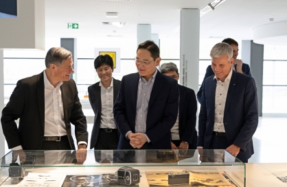
Samsung chief bolsters ties with Germany’s Zeiss
-
7
NewJeans pops out ‘Bubble Gum’ video amid troubles at agency

-
8
Nominee for chief of anti-corruption body pledges 'independence, effectiveness'
-
9
Med schools expect 1,500+ new admission slots next year
-
10
KT launches new mobile plans for foreign residents


Samsung unveils foundry road map to take on TSMC
Tech giant seeks wider adoption of 2nm technology for mobile chips by 2025, automotive chips by 2027
By Jo He-rimPublished : June 28, 2023 - 15:16
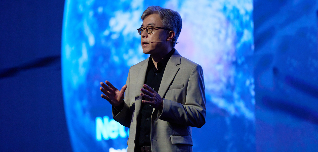
Samsung Electronics, the world’s largest memory chipmaker, on Tuesday unveiled a new foundry business road map, saying it will expand the adoption of the 2-nanometer manufacturing technology in phases to mobile applications by 2025, high-performance computing by 2026 and automotive chips by 2027.
The bold plan comes as Samsung, a distant No. 2 in terms of foundry sales after Taiwan Semiconductor Manufacturing Co., is investing heavily to boost its burgeoning foundry business and narrow the gap with the market leader. According to market tracker TrendForce, Samsung’s foundry market share fell to 12.4 percent in the first quarter of this year, while TSMC further elevated its dominance to 60.1 percent.
“Samsung Foundry has always met customer needs by being ahead of the technology innovation curve and today we are confident that our gate-all-around-based advanced node technology will be instrumental in supporting the needs of our customers using AI applications,” Choi Si-young, president and head of foundry business at Samsung Electronics, said during the Samsung Foundry Forum 2023 held in Silicon Valley, California, Tuesday.
“Ensuring the success of our customers is the most central value to our foundry services.”
Samsung said some 700 representatives of its corporate clients and partners joined the forum held under the theme of “Innovation Beyond Boundaries.”
The tech giant said its 2nm process, called SF2, has shown a 12 percent increase in performance, a 25 percent increase in power efficiency, and a 5 percent decrease in area, when compared to its 3nm process, SF3. The company said it plans to mass-produce the more advanced 1.4nm process in 2027.
From 2025, Samsung will begin foundry services for 8-inch gallium nitride power semiconductors targeting data centers and automotive applications.
In order to secure the most cutting-edge technology in the upcoming 6G network era, Samsung said it is also in the process of developing the 5nm radio frequency for it to be made available in the first half of 2025. Samsung’s 5nm RF process shows a 40 percent increase in power efficiency and a 50 percent decrease in area compared to the previous 14nm process, the company explained.
Introducing the “Shell-First” operation strategy that aims to better respond to customer demands, Samsung said its foundry business will also add new manufacturing lines in Pyeongtaek, Gyeonggi Province, in Korea, and in its Taylor fab in Texas that is currently under construction to begin operation in the second half of 2024.
The expansion plans will increase the company’s clean room capacity by 7.3 times by 2027 when compared to 2021.
Samsung also announced it will begin mass production of foundry products for mobile and other applications at the Pyeongtaek Line 3 facility in the second half of this year.
Samsung's envisioned production base in Yongin, located about 10 kilometers east of the company's Hwaseong and Giheung campuses, will also expand to power the next generation of its foundry services, the company said.
In addition to expanding the application and production, the company said it will also launch an Multi-Die Integration Alliance for next-generation packaging technology involving its partner companies and major players in memory, substrate packaging and testing.
As part of efforts to promote mutual growth of the foundry ecosystem, Samsung said it plans to host the Samsung Advanced Foundry Ecosystem (SAFE) Forum on June 28, bringing together over a hundred partners across electronic design automation, design solution partners, outsourced semiconductor assembly and test, cloud and IP.
“Through extensive collaboration with our SAFE partners, Samsung Foundry is helping simplify designs that are becoming even more complex amid the application of the most advanced processes and new technologies such as heterogeneous integration,” said Kye Jong-wook, executive vice president and head of design platform development under Samsung's foundry business.
“We will continue to strive for consistent growth in the Samsung Foundry ecosystem in terms of both scale and quality.”
Samsung said it will host the Samsung Foundry Forum 2023 in Korea in July as well, and will expand to Europe and Asia later in the year to meet customers in each region.


![[Herald Interview] Mistakes turn into blessings in street performance, director says](http://res.heraldm.com/phpwas/restmb_idxmake.php?idx=652&simg=/content/image/2024/04/28/20240428050150_0.jpg&u=20240428174656)