Most Popular
-
1
40 flights canceled on Jeju Island due to bad weather

-
2
Pandemic left Korea more depressed than before: report

-
3
N. Korea slams US, other countries for seeking alternative to UN sanctions monitoring panel

-
4
Korean labor force to shrink by 10 million by 2044: report

-
5
Gov't appears to shelve punitive measures against mass walkout by doctors


-
6
[AtoZ Korean Mind] Does your job define who you are? Should it?
![[AtoZ Korean Mind] Does your job define who you are? Should it?](//res.heraldm.com/phpwas/restmb_idxmake.php?idx=644&simg=/content/image/2024/05/06/20240506050099_0.jpg&u=)
-
7
Govt. asks hospitals to mitigate impact of medical professors' absence
-
8
S. Korea's working-age population to dip nearly 10m by 2044 amid low births
-
9
Doggy patrol team on the move to protect their cities

-
10
Samsung mocks Apple over iPhone alarm glitch

![[AtoZ Korean Mind] Does your job define who you are? Should it?](http://res.heraldm.com/phpwas/restmb_idxmake.php?idx=644&simg=/content/image/2024/05/06/20240506050099_0.jpg&u=)


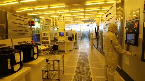
South Korea's ICT ministry said Tuesday a 12-inch semiconductor wafer test bed was established here in line with the country's efforts to boost development of homegrown chip technology.
Previously, the absence of the test bed had led many local small and medium-sized chip component companies to rely on overseas testing facilities, according to the Ministry of Science and ICT.
The country's major chipmakers, such as Samsung Electronics Co. and SK hynix Inc., require evaluations of chip components based on 12-inch wafers.
Since August 2019, the National Nanofab Center has spent 45 billion won ($40 million) to create the test bed, made up of 10 core equipment and a clean room.
The facility will be available for use by companies, universities and research institutes starting Wednesday, according to the ministry.
The move comes as the country looks to boost its reliance on homegrown technology, following a trade dispute with Japan in 2019.
In July that year, Japan imposed tighter regulations on exports of key materials to Seoul, prompting South Korea to wean off reliance on global trade partners and boost local supply chains of technological materials. (Yonhap)