
Most Popular
-
1
1 in 3 Koreans live alone, family types becoming diverse

-
2
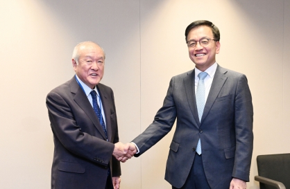
Korea, Japan finance chiefs vow to tame rampant FX market volatility
-
3
US 'incredibly concerned' about suspected NK-Iran military ties

-
4
K-pop group's manager dismissed for setting up spycam in theater dressing room

-
5
K-pop singer lost consciousness after being hit by foul ball, cancels show


![[Kim Seong-kon] Democracy and the future of South Korea](http://res.heraldm.com/phpwas/restmb_idxmake.php?idx=644&simg=/content/image/2024/04/16/20240416050802_0.jpg&u=)


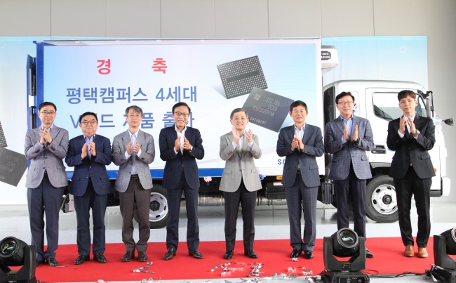
Samsung set to make decision on Pyeongtaek investment
With 40-year knowhow, Samsung to tackle new challenges of making cutting-edge chips
By Song Su-hyunPublished : Feb. 13, 2018 - 16:27
Samsung Electronics’ is set to make an imminent final decision on another round of massive investment -- anticipated at some 30 trillion won ($27.7 billion) -- to expand one of its semiconductor factories into the world’s largest.
Samsung’s new investment is at the center of attention in the global chip industry amid technological challenges and market forecasts of slowing growth this year.
Samsung reportedly held a meeting of its top management on Wednesday last week to discuss the investment to build a second fabrication line in addition to the current NAND flash chip plant in Pyeongtaek, Gyeonggi Province.
The meeting grabbed market attention since it was held two days after Samsung heir Lee Jae-yong was released from a yearlong imprisonment, and raised market expectations that it would lead to swift decision-making.
A day after the meeting, Jin Gyo-young, president of the memory business at Samsung, told reporters that “a final decision on the amount of investment will be made soon.”
Some industry watchers here estimate the upcoming investment would be around 30 trillion won, considering that Samsung invested 27.3 trillion won in building the first line in Pyeongtaek and expanding other facilities last year.
If so, it would exceed market forecasts that Samsung may scale back its spending this year from last year’s record high figure.
A forecast by SEMI Industry Research & Statistics had placed combined fabrication investments by Korean chipmakers -- mostly Samsung -- this year would be around $23 billion.
“Semiconductor investments happen in cycles,” said Jim Handy, CEO and analyst of US-based Objective Analysis at 2018 Semicon Korea held last month.
“Although the market is forecast to see a downturn commencing in the second half of this year, we are hoping to see more investment by Samsung.”
Some others say Samsung’s capital expenditure would continue to mount in the long run in order to overcome technology stalls.
According to a foundry process technology roadmap unveiled by Samsung last year, the chipmaker is set to introduce 7-nanometer, 6-nm, 5-nm and 4-nm process technologies by 2020.
Samsung is aiming to develop the industry’s first 4-nm process, a significant achievement for the Korean company that started 27 years behind its US and Japanese competitors in the industry back in 1974.
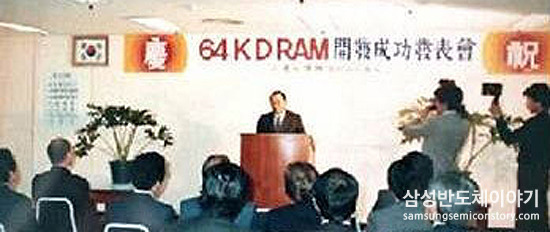
Starting with 64K DRAM that was developed just in six months in 1983, Samsung continued making new records in the global chip industry by announcing the world’s first 64M DRAM in 1992, 256M DRAM in 1994 and 1Gb DRAM in 1996.
To provide smaller but faster memory chips for mobile devices, the company began mass-producing the first three-dimensional NAND flash chips with 24 layers in 2013, and came up with higher layers each year reaching 64 layers so far.
After years of innovation, Samsung’s chipmaking unit secured 40.3 trillion won in operating profit last year, its largest-ever figure.
However, due to the emergence of artificial intelligence, big data and Internet of Things in the fourth industrial revolution era, the kingpin of the chip industry is facing technological challenges in developing higher-speed, lower-power chipsets required for smooth operations of new digital devices.
“As the pace of technology development slows down, production costs may bounce back,” said Kang Ho-kyu, vice president and head of Samsung’s semiconductor R&D center.
“The semiconductor industry will experience the most technological difficulties this year, and close collaboration among chipmakers, equipment providers and material developers is seriously needed.”
By Song Su-hyun (song@heraldcorp.com)
![[KH Explains] Hyundai's full hybrid edge to pay off amid slow transition to pure EVs](http://res.heraldm.com/phpwas/restmb_idxmake.php?idx=652&simg=/content/image/2024/04/18/20240418050645_0.jpg&u=20240418181020)
![[Today’s K-pop] Zico drops snippet of collaboration with Jennie](http://res.heraldm.com/phpwas/restmb_idxmake.php?idx=642&simg=/content/image/2024/04/18/20240418050702_0.jpg&u=)