
Most Popular
-
1
A decade lost: Sewol survivors on life after tragedy

-
2
Opposition victory upends ruling party's plans
-
3
Why don’t trainee doctors, medical professors see eye to eye?
-
4
Taking risk or targeting global fans? Netflix pushes ahead with 'Goodbye Earth' release

-
5
World reactions to Iran strikes on Israel


-
6
S. Korea to extend fuel tax cut through June amid Middle East tensions
-
7
Yoon flounders after election defeat
-
8
Israel says Iran launched more than 300 drones and missiles, 99% of which were intercepted

-
9
US confirms $6.4 billion chip subsidy for Samsung
-
10
N. Korea elevates high-level exchanges with China, Russia


[News Focus] Samsung’s nonmemory plans needs renewed push from Lee
Samsung‘s presence in processor, foundry markets remains weak, but is expected to spur investments with its chief back at the helm
By Song Su-hyunPublished : Aug. 10, 2021 - 18:29
It was Samsung Group’s de facto chief Lee Jae-yong who in 2019 unveiled Samsung Electronics’ whopping 133 trillion won ($155.77 billion) investment plan, in front of President Moon Jae-in, with a vision to grow the presence of the world’s No. 1 memory chip maker in nonmemory fields.
Two years have passed and the Korean chipmaker appears to have made little process on the quest.
With its chief busy fighting criminal charges, including bribery and embezzlement, and being placed behind bars since January this year, the memory-focused Korean chipmaker couldn’t expand into the vast processor chipset market as aggressively as it had planned.
But, with Lee set to be released on parole this Friday, expectations are rising that Samsung’s ambition to have a more balanced chip portfolio could get a renewed push.
A look at Samsung’s second-quarter earnings shows how lopsided its current portfolio is.
Of the 8.2 trillion-won operating profit made from the semiconductor business in the second quarter of this year, the company’s processor chipset and foundry units’ operating profits were estimated to be between 200 billion won and 300 billion won, accounting for less than 2 percent.
The memory business, meanwhile, earned 6.9 trillion won and took over 80 percent of the entire chip business profit.
The latest earnings results showed that Samsung’s reliance on its traditional memory business further increased from two years ago, keeping nonmemory a marginal source of revenue.
“It is true that the company has kind of lost the momentum for the push into the nonmemory market due to the void of leadership,” commented a Samsung senior official.
Although Samsung’s System LSI and Foundry Business, each in charge of processors and customized chip manufacturing services, made doubled efforts to launch new Exynos and ISCOCELL products and technologies, the efforts were confined to the relatively smaller mobile processor market, compared to its US rival Intel that dominates the larger and more expensive central producing unit market.
In the mobile AP market, Samsung‘s market share declined from 14 percent in the first quarter of 2020 to 9 percent in the same quarter this year, according to data by Counterpoint Research. The fall was directly linked to Samsung‘s declines in the smartphone market.
In the foundry sector, Samsung remained second with an 18 percent share, after TSMC with 56 percent in the first quarter, showed data by Statista.
To gain a stronger foothold in nonmemory, Samsung needs to chip away at the market shares of TSMC and Intel.
Samsung‘s announcement on Tuesday of the launch of a wearable processor Exynos W920 -- the tiniest chipset but with a 20 percent improvement in performance -- was one of outcomes the company is continuing to produce in the processor market.
Samsung System LSI also drew attention with its plan for development of neural processing unit, known as the “brain of AI,“ and the industry‘s first multimode 5G chipset.
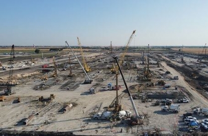
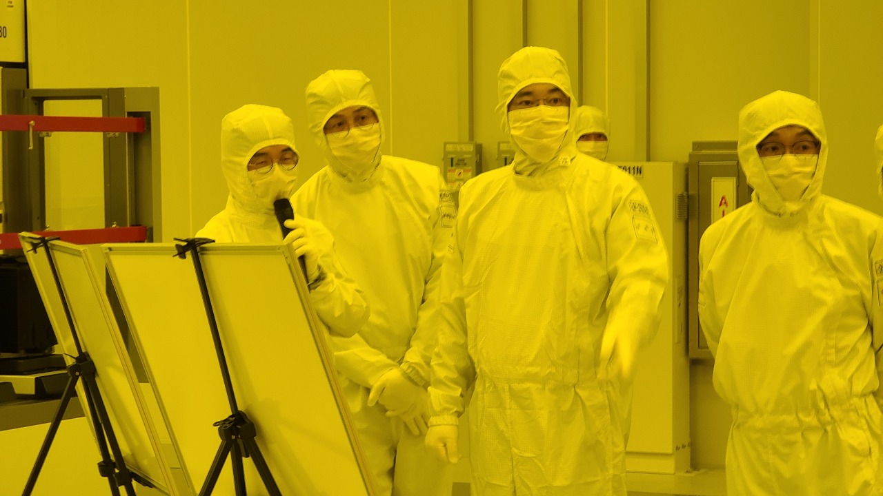
The company is currently constructing the third plant of its Pyeongtaek campus, the P3, which will be equipped with the most advanced extreme ultraviolet lithography equipment for customized manufacturing on 5-nanometer and lower processes. The P3 fab, slated for operation 2022, was planned to narrow the gap with TSMC in the foundry market.
“Samsung takes about 40 percent of a particular sector of the foundry market for 10-nm processes and below, owing to the efforts to take down TSMC in the market that requires more advanced technologies,“ explained a Samsung spokesperson.
According to industry officials, Lee’s release would accelerate Samsung’s decision-making for major investments in the field, although his business activities wouldn’t be as active as before due to the five-year employment ban that is expected to be maintained despite the parole decision.
Besides the company’s plan for a $18 billion foundry plant in the US, Samsung is expected to announce a remarkably-sized acquisition that could change the order of the nonmemory market.
Before Lee’s imprisonment, Samsung was rumored to be examining M&A targets, including automotive chipmakers like NXP from the Netherlands or 5G chip developer Xilinx from the US.
“Samsung may eye a target that has specialty in the fields of autonomous driving, artificial intelligence and biotechnology to secure new technologies through an M&A,” said an industry observer.
US investment bank JP Morgan still forecasts that there remains room for Samsung to consider the acquisition of NXP that could value over 70 trillion won.
In May, Samsung announced it will further increase the investments in the system chip and foundry businesses up to 171 trillion won, and confirmed that it is preparing for a significant M&A deal to realize the goal of being the top of the whole semiconductor market.
“There was no major investment announcement while Lee was in jail, but Samsung seemed to be working on its nonmemory vision in various ways,” said Kim Yang-paeng, senior research fellow at Korea Institute for Industry and Economics. “The company has the potential to further strengthen its nonmemory businesses by reinforcing its current logic chips with its cutting-edge technologies using EUV and integration with memory solutions, as well as image sensors.”
Two years have passed and the Korean chipmaker appears to have made little process on the quest.
With its chief busy fighting criminal charges, including bribery and embezzlement, and being placed behind bars since January this year, the memory-focused Korean chipmaker couldn’t expand into the vast processor chipset market as aggressively as it had planned.
But, with Lee set to be released on parole this Friday, expectations are rising that Samsung’s ambition to have a more balanced chip portfolio could get a renewed push.
A look at Samsung’s second-quarter earnings shows how lopsided its current portfolio is.
Of the 8.2 trillion-won operating profit made from the semiconductor business in the second quarter of this year, the company’s processor chipset and foundry units’ operating profits were estimated to be between 200 billion won and 300 billion won, accounting for less than 2 percent.
The memory business, meanwhile, earned 6.9 trillion won and took over 80 percent of the entire chip business profit.
The latest earnings results showed that Samsung’s reliance on its traditional memory business further increased from two years ago, keeping nonmemory a marginal source of revenue.
“It is true that the company has kind of lost the momentum for the push into the nonmemory market due to the void of leadership,” commented a Samsung senior official.
Although Samsung’s System LSI and Foundry Business, each in charge of processors and customized chip manufacturing services, made doubled efforts to launch new Exynos and ISCOCELL products and technologies, the efforts were confined to the relatively smaller mobile processor market, compared to its US rival Intel that dominates the larger and more expensive central producing unit market.
In the mobile AP market, Samsung‘s market share declined from 14 percent in the first quarter of 2020 to 9 percent in the same quarter this year, according to data by Counterpoint Research. The fall was directly linked to Samsung‘s declines in the smartphone market.
In the foundry sector, Samsung remained second with an 18 percent share, after TSMC with 56 percent in the first quarter, showed data by Statista.
To gain a stronger foothold in nonmemory, Samsung needs to chip away at the market shares of TSMC and Intel.
Samsung‘s announcement on Tuesday of the launch of a wearable processor Exynos W920 -- the tiniest chipset but with a 20 percent improvement in performance -- was one of outcomes the company is continuing to produce in the processor market.
Samsung System LSI also drew attention with its plan for development of neural processing unit, known as the “brain of AI,“ and the industry‘s first multimode 5G chipset.
The company is currently constructing the third plant of its Pyeongtaek campus, the P3, which will be equipped with the most advanced extreme ultraviolet lithography equipment for customized manufacturing on 5-nanometer and lower processes. The P3 fab, slated for operation 2022, was planned to narrow the gap with TSMC in the foundry market.
“Samsung takes about 40 percent of a particular sector of the foundry market for 10-nm processes and below, owing to the efforts to take down TSMC in the market that requires more advanced technologies,“ explained a Samsung spokesperson.
According to industry officials, Lee’s release would accelerate Samsung’s decision-making for major investments in the field, although his business activities wouldn’t be as active as before due to the five-year employment ban that is expected to be maintained despite the parole decision.
Besides the company’s plan for a $18 billion foundry plant in the US, Samsung is expected to announce a remarkably-sized acquisition that could change the order of the nonmemory market.
Before Lee’s imprisonment, Samsung was rumored to be examining M&A targets, including automotive chipmakers like NXP from the Netherlands or 5G chip developer Xilinx from the US.
“Samsung may eye a target that has specialty in the fields of autonomous driving, artificial intelligence and biotechnology to secure new technologies through an M&A,” said an industry observer.
US investment bank JP Morgan still forecasts that there remains room for Samsung to consider the acquisition of NXP that could value over 70 trillion won.
In May, Samsung announced it will further increase the investments in the system chip and foundry businesses up to 171 trillion won, and confirmed that it is preparing for a significant M&A deal to realize the goal of being the top of the whole semiconductor market.
“There was no major investment announcement while Lee was in jail, but Samsung seemed to be working on its nonmemory vision in various ways,” said Kim Yang-paeng, senior research fellow at Korea Institute for Industry and Economics. “The company has the potential to further strengthen its nonmemory businesses by reinforcing its current logic chips with its cutting-edge technologies using EUV and integration with memory solutions, as well as image sensors.”