
Most Popular


![[KH Explains] How should Korea adjust its trade defenses against Chinese EVs?](http://res.heraldm.com/phpwas/restmb_idxmake.php?idx=644&simg=/content/image/2024/04/15/20240415050562_0.jpg&u=20240415144419)


Samsung embarks on NAND flash line at 2nd Pyeongtaek fab
Chipmaker pours W8tr more this year to address future memory demand
By Song Su-hyunPublished : June 1, 2020 - 15:04

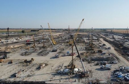
Samsung Electronics announced Monday it has embarked on creating the second production line for its advanced V-NAND flash memory chips in Pyeongtaek, Gyeonggi Province, with a schedule to start rolling them out in the second half of 2021.
The company has started working on the NAND cleanroom in May in order to respond to the rising demand for artificial intelligence and internet of things technologies amid the spreading non-contact lifestyles and services in the wake of the COVID-19 outbreak.
The latest investment in the new NAND fab is estimated to be around 8 trillion won ($6.5 billion), according to industry sources.
It is the second large-scale investment plan announced by Samsung last month. On May 21, the firm said it will break ground for the second extreme ultraviolet foundry line in the same region with a schedule to start operating the new line in the second half of next year with an investment of 10 trillion won.
According to industry sources, Samsung is also planning to announce another 15 trillion won worth DRAM EUV line at the second fab in the near future.
The Pyeongtaek campus was completed in 2015, marking the world’s biggest semiconductor production complex. The first fab has been mass-producing NAND on the first floor and DRAMs on the second floor.
It appears the chipmaker will start churning out DRAMs using extreme ultraviolet lithography at the second fab within the year, while pushing the schedule for NAND production to next year, according to industry watchers.
Last month, one Samsung C&T employee working for the construction of the second Pyeongtaek fab tested positive for the coronavirus, halting work for days.
Samsung was the world’s largest NAND flash provider with a 33.3 percent market share as of the first quarter, according to data by TrendForce.
Since it announced its first-generation 24-layer 128-Gigabit MLC 3D V-NAND in July 2013, Samsung has continued revolutionizing NAND technologies for the last six years. In 2019, it started mass-producing the latest sixth-generation NAND with over 100 layers.
“The new investment reaffirms our commitment to sustain undisputed leadership in memory technologies, even in uncertain times,” said Cheol Choi, executive vice president of memory global sales and marketing at Samsung.
“We will continue to serve the market with the most optimized solutions available, while contributing to growth of the overall IT industry and the economy in general.”
By Song Su-hyun (song@heraldcorp.com)


![[Today’s K-pop] Stray Kids to return soon: report](http://res.heraldm.com/phpwas/restmb_idxmake.php?idx=642&simg=/content/image/2024/04/16/20240416050713_0.jpg&u=)