
Most Popular
-
1
[Exclusive] Korean military set to ban iPhones over 'security' concerns
![[Exclusive] Korean military set to ban iPhones over 'security' concerns](//res.heraldm.com/phpwas/restmb_idxmake.php?idx=644&simg=/content/image/2024/04/23/20240423050599_0.jpg&u=20240423183955)
-
2
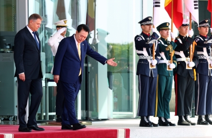
Korean, Romanian leaders discuss defense tech, nuclear energy
-
3
[Graphic News] 77% of young Koreans still financially dependent
![[Graphic News] 77% of young Koreans still financially dependent](//res.heraldm.com/phpwas/restmb_idxmake.php?idx=644&simg=/content/image/2024/04/22/20240422050762_0.gif&u=)
-
4
S. Korea calls on Japan to confront history amid Yasukuni Shrine visit

-
5
Yoon’s jailed mother-in-law excluded from latest parole list

![[Exclusive] Korean military set to ban iPhones over 'security' concerns](http://res.heraldm.com/phpwas/restmb_idxmake.php?idx=644&simg=/content/image/2024/04/23/20240423050599_0.jpg&u=20240423183955)

![[Graphic News] 77% of young Koreans still financially dependent](http://res.heraldm.com/phpwas/restmb_idxmake.php?idx=644&simg=/content/image/2024/04/22/20240422050762_0.gif&u=)


-
6
Hybe and Min Hee-jin, CEO of Hybe sublabel Ador, lock horns

-
7
[Pressure points] Leggings in public: Fashion statement or social faux pas?
![[Pressure points] Leggings in public: Fashion statement or social faux pas?](//res.heraldm.com/phpwas/restmb_idxmake.php?idx=644&simg=/content/image/2024/04/23/20240423050669_0.jpg&u=)
-
8
Yoo Jae-suk, Yoo Yeon-seok team up in 'Whenever Possible'

-
9
Korea’s homegrown nanosatellite successfully launches into space

-
10
Aging population to drive down Korea's housing prices from 2040: experts

![[Pressure points] Leggings in public: Fashion statement or social faux pas?](http://res.heraldm.com/phpwas/restmb_idxmake.php?idx=644&simg=/content/image/2024/04/23/20240423050669_0.jpg&u=)


Samsung heir discusses world’s first 3-nm process for foundry
By Song Su-hyunPublished : Jan. 2, 2020 - 17:27
Samsung Electronics’ de facto leader Lee Jae-yong on Thursday discussed the tech giant’s strategy to utilize the world’s first 3-nanometer process technology for manufacturing chips.
Lee visited the company’s semiconductor research and development center in Hwaseong, Gyeonggi Province, as his first official gesture of on-site management in 2020.
The Samsung heir discussed the company’s plans to commercialize cutting-edge chips ordered from global customers on the latest 3-nm gate-all-around process technology under development, according to the firm.

GAA is known as an architectural successor to the current FinFET technology, which enables chipmakers to push further the nanometer range for microchips.
Samsung completed the development of a 5-nm FinFET process tech based on extreme ultraviolet technologies in April last year. And it is working on the next-generation nanometer process tech.
Compared with the 5-nm process, the 3-nm GAA tech provides an increase of more than 35 percent in logic area efficiency with 50 percent lower power consumption and about 30 percent higher performance, the company said.
“Lee’s visit to the semiconductor R&D center once again highlights Samsung’s pledge to grow as a top chipmaker in the non-memory field,” said a Samsung spokesman.
Last year, Samsung announced a 133 trillion won ($111.85 billion) investment plan with the goal of becoming the world’s top maker of systems on chips by 2030.
By Song Su-hyun (song@heraldcorp.com)