

Most Popular


-
6
[Graphic News] More Koreans say they plan long-distance trips this year
![[Graphic News] More Koreans say they plan long-distance trips this year](//res.heraldm.com/phpwas/restmb_idxmake.php?idx=644&simg=/content/image/2024/04/17/20240417050828_0.gif&u=)
-
7
[KH Explains] Hyundai's full hybrid edge to pay off amid slow transition to pure EVs
![[KH Explains] Hyundai's full hybrid edge to pay off amid slow transition to pure EVs](//res.heraldm.com/phpwas/restmb_idxmake.php?idx=644&simg=/content/image/2024/04/18/20240418050645_0.jpg&u=20240419100350)
-
8
North Korea removes streetlights along cross-border roads with South

-
9
Russia's denial of entry of S. Korean national unrelated to bilateral ties: Seoul official

-
10
Farming households dip below 1m for first time in 2023

![[Graphic News] More Koreans say they plan long-distance trips this year](http://res.heraldm.com/phpwas/restmb_idxmake.php?idx=644&simg=/content/image/2024/04/17/20240417050828_0.gif&u=)
![[KH Explains] Hyundai's full hybrid edge to pay off amid slow transition to pure EVs](http://res.heraldm.com/phpwas/restmb_idxmake.php?idx=644&simg=/content/image/2024/04/18/20240418050645_0.jpg&u=20240419100350)


Samsung is moving to strengthen its foundry business by adding a new 11-nanometer FinFET process technology and developing the industry’s first 7-nm process tech, the company announced Monday.
By adding the 11-nm FinFET process, Samsung now has wider range of options for their next-generation products in terms of cost effectiveness.
Also known as the 11 Lower Power Plus (11LPP) process, the cutting-edge tech delivers up to 15 percent higher performance and 10 percent chip area reduction with the same power consumption, the company said.
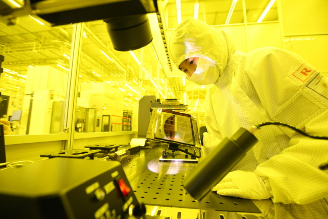
Samsung is currently producing mobile processors for premium smartphones with the most advanced 10-nm FinFET process. The addition of the 11-nm process that charges relatively lower cost than 10-nm process is targeted for mid- and low-end smartphone makers.
Samsung is under development of the industry’s first 7-nm process with extreme ultra violet (EUV) lithography technology with an aim to apply the tech to mass-producing chips starting the second half of next year, it said.
The company has tried processing nearly 200,000 wafers with the EUV lithography tech since 2014, and has recently achieved 80 percent in yields for production of 256-megabit static random-access memory chips.
Details of the recent update to Samsung’s foundry roadmap, including 11LPP availability and 7nm EUV development, will be elaborated at the Samsung Foundry Forum Japan this Friday in Tokyo.
The world’s No.1 memory chipmaker has completed a process roadmap spanning from 14-nm to 11-nm, 10-nm, 8-nm and 7-nm for the next three years.
By Song Su-hyun (song@heraldcorp.com)


![[KH Explains] Hyundai's full hybrid edge to pay off amid slow transition to pure EVs](http://res.heraldm.com/phpwas/restmb_idxmake.php?idx=652&simg=/content/image/2024/04/18/20240418050645_0.jpg&u=20240419100350)

![[Today’s K-pop] Illit drops debut single remix](http://res.heraldm.com/phpwas/restmb_idxmake.php?idx=642&simg=/content/image/2024/04/19/20240419050612_0.jpg&u=)