

Most Popular
-
1
Korea’s homegrown nanosatellite successfully launches into space

-
2
[Herald Interview] 'Amid aging population, Korea to invite more young professionals from overseas'
![[Herald Interview] 'Amid aging population, Korea to invite more young professionals from overseas'](//res.heraldm.com/phpwas/restmb_idxmake.php?idx=644&simg=/content/image/2024/04/24/20240424050844_0.jpg&u=20240424200058)
-
3
Nicaragua shuts down Seoul embassy

-
4
Hybe's multilabel system tested amid conflict with Ador

-
5
Ador CEO denies allegations, accuses Hybe of mistreating NewJeans


![[Herald Interview] 'Amid aging population, Korea to invite more young professionals from overseas'](http://res.heraldm.com/phpwas/restmb_idxmake.php?idx=644&simg=/content/image/2024/04/24/20240424050844_0.jpg&u=20240424200058)


-
6
Rocket engine expert, ex-NASA exec to lead Korea's new space agency
-
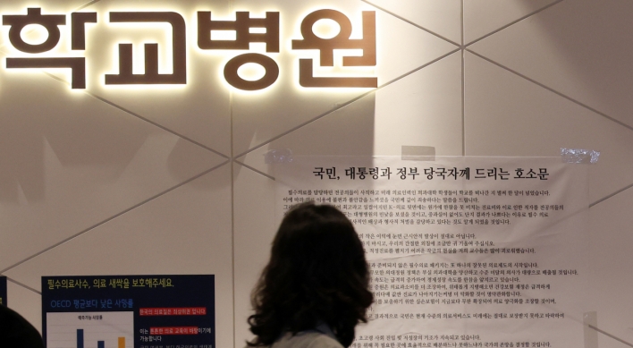
7
SNU profs to suspend treatment for one day
-
8
SK hynix pledges W20tr to ramp up DRAM production at home
-
9
Over-50s, men, single-person households take up majority of those filing for bankruptcy

-
10
Pianist Cho Seong-Jin named Berlin Philharmonic's artist-in-residence


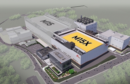
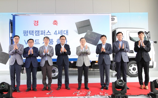
Samsung kick-starts new NAND chip plant in Pyeongtaek
By Korea HeraldPublished : July 4, 2017 - 15:38
The world’s biggest memory chip provider Samsung Electronics announced Tuesday the company had officially started operation of its newest semiconductor fabrication line in Pyeongtaek, Gyeonggi Province, along with 37 trillion won ($32.2 billion) worth of investment plans by 2021.
The new line is the largest single fabrication line in the entire industry. It took about two years of construction after breaking ground in May 2015 with a total of 15.6 trillion won worth of investment.
The facility will focus on the production of Samsung’s fourth-generation 64-layer V-NAND chips, adding to the company’s capacity for cutting-edge memory products, the firm said.

Demand for 64-layer V-NAND chips is growing at an explosive rate due to the recent trends of the Internet of Things, artificial intelligence, big data and connected vehicles.
NAND flash memory is a type of nonvolatile storage medium that does not require power to retain data. Samsung’s fourth-generation V-NAND is 3-D and stacks 64 layers of cells to store up to 256 gigabits of data. The higher the number of layers, the more the data can be stored at a faster data processing speed. Compared to its predecessor 48-layer NAND chips, the 64-layer NAND chips have a 30 percent increase in productivity.
Mass production of the latest V-NAND chips at the new plant is part of Samsung’s strategy to focus its capacities on the growing NAND chip market that is estimated to expand nearly 40 percent every year.
It had been providing the chips confidentially to a selected number of customers since late last year, but had put off their mass production until the completion of the new Pyeongtaek fabrication line.
The company held an internal ceremony to mark the start of the mass production with the attendance of around 100 executives.
“With the dedication and support of our employees, customers and partners, our new Pyeongtaek campus represents a new chapter in Samsung’s semiconductor operations,” said Kwon Oh-hyun, vice chairman and CEO of Samsung Electronics, at the ceremony.
In response to rising market needs, Samsung, across both Samsung Electronics and Samsung Display, plans to reinforce its manufacturing capabilities by investing more than 37 trillion won into its global production facilities.
Samsung will invest a total of 30 trillion won into its current Pyeongtaek line to expand its fabrication capacity by 2021.
The company also plans to invest 6 trillion won in its Hwaseong plant, also in Gyeonggi Province, to install cutting-edge manufacturing equipment, including extreme ultraviolet equipment, it said.
Samsung Display is reviewing plans to establish a new organic light-emitting diode manufacturing site in Asan, South Chungcheong Province, by 2018.
The new domestic investments are forecast to create a total of 163 trillion won worth of economic effects and 440,000 new jobs, according to data from the Bank of Korea.
The Korean semiconductor leader is also considering a plan to construct its second chip plant in Xi’an, China, in addition to its first one built in 2014, it said. The first Xi’an plant is currently producing NAND chips.
By Song Su-hyun (song@heraldcorp.com)
-
Articles by Korea Herald


![[KH Explains] Korean shipbuilding stocks rally: Real growth or bubble?](http://res.heraldm.com/phpwas/restmb_idxmake.php?idx=652&simg=/content/image/2024/04/25/20240425050656_0.jpg&u=)