
Most Popular
-
1
[Herald Interview] 'Amid aging population, Korea to invite more young professionals from overseas'
![[Herald Interview] 'Amid aging population, Korea to invite more young professionals from overseas'](//res.heraldm.com/phpwas/restmb_idxmake.php?idx=644&simg=/content/image/2024/04/24/20240424050844_0.jpg&u=20240424200058)
-
2
Korea’s homegrown nanosatellite successfully launches into space

-
3
Nicaragua shuts down Seoul embassy

-
4
Rocket engine expert, ex-NASA exec to lead Korea's new space agency
-
5
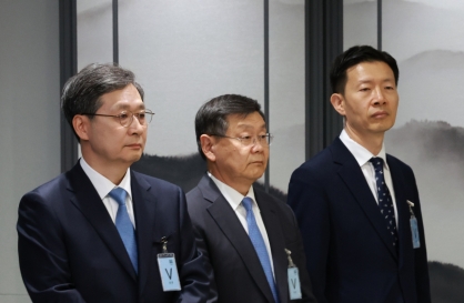
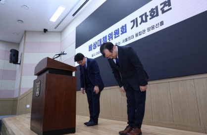
SNU profs to suspend treatment for one day
![[Herald Interview] 'Amid aging population, Korea to invite more young professionals from overseas'](http://res.heraldm.com/phpwas/restmb_idxmake.php?idx=644&simg=/content/image/2024/04/24/20240424050844_0.jpg&u=20240424200058)


-
6
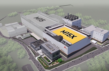
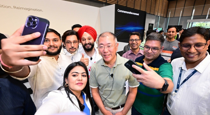
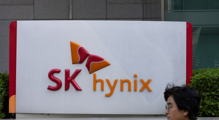
SK hynix pledges W20tr to ramp up DRAM production at home
-
7
Hybe's multilabel system tested amid conflict with Ador

-
8
Over-50s, men, single-person households take up majority of those filing for bankruptcy

-
9
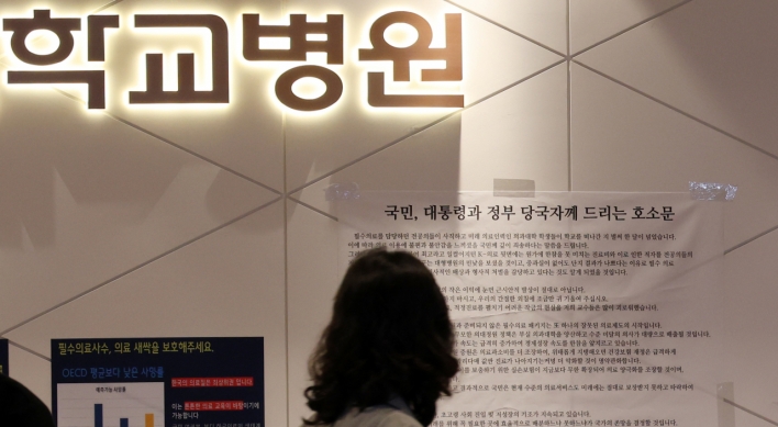
Ministry denies blame for Jamboree debacle

-
10
Pianist Cho Seong-Jin named Berlin Philharmonic's artist-in-residence


Samsung Electro-Mechanics to invest W263b in chip technology
By Kim Young-wonPublished : July 22, 2016 - 15:23
[THE INVESTOR] Electronic components firm Samsung Electro-Mechanics said on July 22 that it would invest 263.2 billion won (US$231.90 million) in beefing up its capability in chip packaging, an encapsulation process aimed at preventing erosion and damage.
The investment amount accounts for 6.1 percent of the firm’s equity.

Through the investment, Samsung Electro-Mechanics will develop the next-generation chip packaging facilities, which will be deployed at Samsung Display’s manufacturing complex in Cheonan, South Chungcheong Province.
Teaming up with Samsung Electronics’ system LSI division, in charge of developing non-memory chips such as application processors, the electronic components firm will start a project to develop the fan-out wafer level package or FoWLP technology, which can reduce the size of a chip and production cost in a dramatic manner.
Thanks to an upper hand in its own FoWLP technology, TSMC, a Taiwanese chip foundry firm, was able to strike a supply deal of mobile application processor for Apple’s next iPhones.
By Kim Young-won (wone0102@heraldcorp.com)

![[Today’s K-pop] Kep1er to disband after 2 1/2 years: report](http://res.heraldm.com/phpwas/restmb_idxmake.php?idx=642&simg=/content/image/2024/04/25/20240425050792_0.jpg&u=)