Most Popular
-
1
Korea’s homegrown nanosatellite successfully launches into space

-
2
[Herald Interview] 'Amid aging population, Korea to invite more young professionals from overseas'
![[Herald Interview] 'Amid aging population, Korea to invite more young professionals from overseas'](//res.heraldm.com/phpwas/restmb_idxmake.php?idx=644&simg=/content/image/2024/04/24/20240424050844_0.jpg&u=20240424200058)
-
3
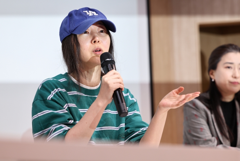
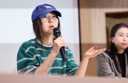
Ador CEO denies allegations, accuses Hybe of mistreating NewJeans
-
4
Nicaragua shuts down Seoul embassy

-
5
Hybe's multilabel system tested amid conflict with Ador

![[Herald Interview] 'Amid aging population, Korea to invite more young professionals from overseas'](http://res.heraldm.com/phpwas/restmb_idxmake.php?idx=644&simg=/content/image/2024/04/24/20240424050844_0.jpg&u=20240424200058)


-
6
Rocket engine expert, ex-NASA exec to lead Korea's new space agency
-
7
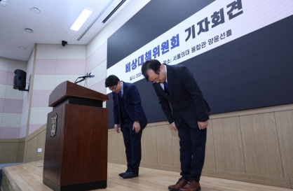
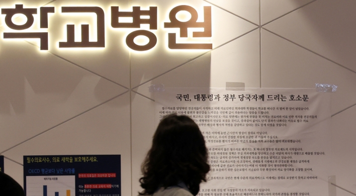
SNU profs to suspend treatment for one day
-
8
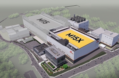
SK hynix pledges W20tr to ramp up DRAM production at home
-
9
Over-50s, men, single-person households take up majority of those filing for bankruptcy

-
10
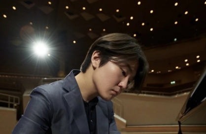
Pianist Cho Seong-Jin named Berlin Philharmonic's artist-in-residence


“삼성전자 사장 (이재용)을 포함한 임원들 모두 산호세 신사옥이 새로운 혁신을 가져오리라는 기대를 가지고 주목하고 있다.”
실리콘 밸리의 심장에 위치한 산호세시에 새롭게 지어질 삼성전자의 반도체 본부의 디자인을 맡은 NBBJ의 디자인 파트너 조나단 워드의 말이다.
코리아 헤럴드와의 인터뷰에서 그는 이번 프로젝트에 대해 안팎으로 기대가 크다는 점을 강조하며, 삼성과의 파트너쉽에 대해 입을 열었다.
“한국기업들은 사실 같이 일하기 어려운 면이 많다. 무엇보다 스케쥴에 대한 압박이 큰 편이다,” 라는 워드는 그럼에도 한국을 사랑할 수밖에 없는 이유는 한국인들은 누구보다 다이내믹하고 새로운 것에 대한 호기심이 많이 때문이라고 했다.
워드는 이번 산호세 신사옥외에도 수원에 위치한 R5 연구소도 디자인했다. 한국기업들 중에는 NHN과도 인연이 있으며, LG등의 새로운 기업도 언제든지 환영한다고 했다.
이번 산호세 프로젝트는 무엇보다 애플과 또 다른 경쟁의 시작이라는 점에서 더욱 주목을 끌고 있다.
현재 삼성과 소송중인 애플도 쿠퍼티노 사옥을 확장할 예정이며, 규모는 약 2만 명의 직원을 수용할 정도로 예상되고 있다. 무엇보다, 스티브 잡스의 유언대로 혁신에 혁신을 더한 디자인이 아니겠냐는 루머가 무성하다.
이 때문에 산호세의 삼성 직원간에도 애플 신사옥과 비교했을 때 결코 뒤지지 않았으면 하는 생각이 강한 것으로 보였다.
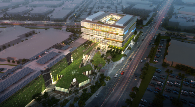
산호세 본부는 2층짜리 건물 여러 개를 켜켜이 쌓아 올린 형태로, 반도체 웨이퍼 (얇은 실리콘 판)를 본떴다.
“쌓아 올린 층 사이사이마다 기술과 전산능력을 갖춘 반도체 웨이퍼와 같이, 직원들간의 긴밀한 협력과 소통을 생각한 디자인,” 이라는 것이 워드의 설명이다.
이 연결성은 중앙의 정원이 완성한다. 겉에서 봤을 때는 조심스럽게 차곡차곡 쌓아 올린 건물의 모습이지만, 위에서 들여다 봤을 때 정가운데가 모두 정원으로 꾸며질 예정이다.
직원들이 각자의 사무실에서 나와 다른 장소로 이동할 때도 정원을 통하고, 식사를 하고 산책을 하기도 하며, 무엇보다 소통의 장으로 활용할 할 수 있도록 디자인된 것이다.
비용은 약 3억불 가량 소요될 예정이며, 총 10층의 높이에 약 2,000명의 인력을 수용할 수 있도록 지어질 산호세 사옥은 지난 7월에 착공식을 가졌다. (코리아 헤럴드 김지현/신지혜 기자)
<관련 영문 기사>
Samsung seeks evolution with new Silicon Valley base
The grandiose plans for constructing Samsung’s new headquarters in Silicon Valley’s heart of San Jose are underway, and designer Jonathan Ward spoke to The Korea Herald about the $300 million project and his client, Samsung.
“The CEO (Samsung’s Lee Jay-yong) in Seoul and all of San Jose’s Samsung executives have been very excited and supportive and are looking forward to seeing how this new building can evolve and transform their culture in the hotbed of Silicon Valley,” said Ward, who is a partner at global architect firm NBBJ.
Those close to Samsung here said the San Jose building would inevitably add fuel to the rivalry between the Korean tech giant and Apple Inc., which is gearing up to open a new campus by 2016. The Apple 2 Campus is expected to be huge, not to mention innovative and quintessentially Apple, but the details have yet to be finalized.
“We’re fighting for the top spot in the industry, so we might as well have it out again, this time in the race to build the better office facility,” said one Samsung R&D official, declining to be identified. He added that his views did not reflect company policy.
Aware of the pressure, Samsung handpicked Ward and NBBJ after seeing the design for Samsung Electronics Learning Center, which was never built but made the Korean firm take notice.
Eventually, Ward wound up designing the R5 center in Suwon, Gyeonggi Province, another facility that won kudos for being both aesthetically pleasing and highly functional as an R&D center housing Samsung employees from all over the world.
Creativity, inspiration and modernity were the key terms Ward grappled with when designing the San Jose building as he was acutely conscious of growing criticism of Silicon Valley’s lack of architectural finesse, which ran counter to its reputation as home to the world’s most innovative enterprises.
In the end, the design for the new facility was inspired by none other than one of Samsung’s best-selling products: semiconductors.
“The idea here was developed initially from the idea of using the building to help generate greater synergy between the employees at Samsung. The semiconductor does something similar ― it is a series of layers and wafers with gases in between each layer that enables high-speed communication and computation,” Ward said.
Two-story buildings were stacked on top of each other for this “chip effect.” This design innovation is not so blatant from the facade, but a glimpse from the rooftop reveals that a courtyard is nestled between the buildings to link them together and offer ample green scenery to the workers.
“Each employee is no more than one floor from the outdoors, and the gardens and courtyard enable interaction, chance encounters and synergy. ... So back to the semiconductor wafer!” Ward said.
Employees can chat, snack or go for a stroll in the gardens that are easily accessible from anywhere in the edifice.
Creating a look unlike anything from Samsung’s rivals was another challenge.
“The San Jose project required a unique solution that sets Samsung apart from Apple, Google, Nvidia and others, makes a creative statement about Samsung and makes a unique, fun and effective workplace for the future of Samsung,” the designer explained.
Stressing his love for Korea, the people and culture, the designer noted that Korean clients were very curious and interested in new ideas, but also quite demanding in terms of timetables.
NHN is among NBBJ’s Korean clients, and Ward said he looked forward to contracts with others such as LG in the future.
Set to open in 2015, the San Jose facility broke ground in July. It will be comprised of a 10-story tower, an amenity pavilion and parking garage. The exterior is to be chiefly white metal, glass and terracotta, while the parking structure will be covered in a folding green-colored wall.
Up to 2,000 employees will work in the tower, which will house both R&D and sales departments.
For greater energy-efficiency, a rooftop solar array on the parking garage will deliver renewable energy, and clear glass will be used to allow natural light to seep deeper into the floor plates, NBBJ said.
By Kim Ji-hyun and Shin Ji-hye
(jemmie@heraldcorp.com) (shinjh@heraldcorp.com)
![[KH Explains] Korean shipbuilding stocks rally: Real growth or bubble?](http://res.heraldm.com/phpwas/restmb_idxmake.php?idx=652&simg=/content/image/2024/04/25/20240425050656_0.jpg&u=)